India Semiconductor Mission (ISM) UPSC
It is a component of a larger initiative to create a nationwide semiconductor and display ecosystem that is sustainable. The program's goal is to give businesses that invest in semiconductor, display manufacturing, and design ecosystems financial support.
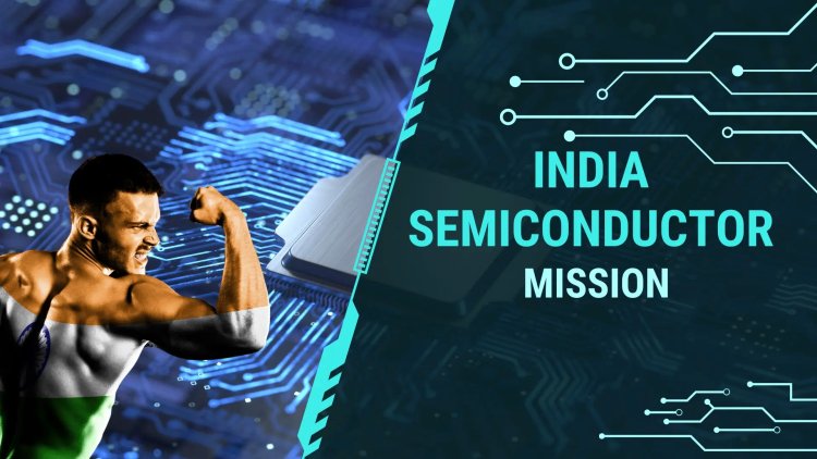
India Semiconductor Mission (ISM)
The Design-Linked Incentive (DLI) program, a crucial component of the "Indian Semiconductor Mission" (ISM), is about to undergo its mid-term evaluation. Only seven of the program's intended 100 start-ups over a five-year period have been approved, prompting calls for a re-evaluation and potential rebirth of the initiative.
India hopes to become a worldwide center for semiconductors, but the scarcity of semiconductor chips has brought attention to supply chain weaknesses and underscored the need for expanding domestic production capacity.
Semiconductor
- Any type of crystalline solids with an electrical conductivity that falls in between that of conductors and insulators is referred to as a semiconductor.
- Several electrical devices, such as integrated circuits (ICs), diodes, and transistors, are made using semiconductors. These devices' low cost, energy efficiency, compact size, and dependability make them widely used.
- As separate components, they are utilized in power devices, optical sensors, and light emitters, such as solid-state lasers.
- Crystalline materials with four valence electrons on average make up semiconductors. Two typical elemental semiconductors used in electronic devices are silicon and germanium.
Introduction of the India Semiconductor Mission (ISM)
- Under the auspices of the Ministry of Electronics and Information Technology (MeitY), ISM was introduced in 2021 at a cost of Rs 76,000 crore.
- It is a component of a larger initiative to create a nationwide semiconductor and display ecosystem that is sustainable.
- The program's goal is to give businesses that invest in semiconductor, display manufacturing, and design ecosystems financial support.
- ISM is expected to serve as the central organization for the effective, cohesive, and seamless execution of the plans, guided by international specialists in the semiconductor and display sectors.

India Semiconductor Mission (ISM) - Component:
- The idea to establish semiconductor factories in India
- Aim to establish display factories in India
- Plan for establishing semiconductor assembly, testing, marking, and packaging (ATMP)/OSAT facilities in India as well as compound semiconductor, silicon photonics, and sensor fabrication facilities.
Scheme for Design-Linked Incentive (DLI):
First of all, At different phases of development and implementation, it offers financial incentives for integrated circuits (ICs), chipsets, systems on chips (SoCs), semiconductor designs for IP Cores and systems, and other semiconductor-linked concepts. offers assistance for the infrastructure.
Nodal Agency: The scientific society C-DAC (Centre for Development of Advanced Computing), which is governed by MeitY, will serve as the nodal agency for carrying out the DLI program.
Three DLI components are as follows:
Support for Chip Design Infrastructure: In order to host cutting-edge design infrastructure (including IP cores, EDA tools, multi-project wafer fabrication/MPW, and post-silicon validation), C-DAC will establish a "India Chip Center." It will also grant sponsored enterprises access to this infrastructure. will provide easy access to it.
Product Design Linked Incentive: Under this, qualified applicants working on semiconductor design will receive financial help in the form of reimbursement of up to 50% of the eligible expenditure, up to a maximum of Rs 15 crore per application.
Deployment Linked Incentive:
Under this, approved applicants whose integrated circuits (ICs), chipsets, semiconductor designs of Systems on Chips (SoCs), system & IP Cores, and semiconductor-linked designs are used in electronic products will receive an incentive ranging from 6% to 4% of net sales turnover over five years, subject to a maximum of Rs 30 crore per application.
Vision: To establish a thriving ecosystem for semiconductor and display design and innovation so that India can become a major global center for electronics design and manufacture.
Importance: Organizing initiatives to promote the semiconductor and display industries in a more structured, targeted, and all-encompassing way requires the involvement of ISM.
What's Your Reaction?